 HrZZ - UIP-2020-02-8891HrZZ - UIP-2020-02-8891HrZZ - UIP-2020-02-8891
MOBDOL-2023-08-2165
The MOBDOL grant focuses on functionalizing TMDs with organic molecules using UHV-STM as the primary characterization tool, complemented by AFM and Raman spectroscopy under ambient conditions.
During the first period of the grant (03/2024 – 01/2025), efforts were dedicated to establishing key experimental protocols essential for achieving the project’s final objectives in the second period. This phase included the growth of graphene-covered metal substrates—Ir(111), Ir(332), and Ni(111)—for future TMD deposition (see Figure 01). These substrates were specifically chosen to tailor the properties of the TMD layers grown on them. Once the growth protocols were established, we investigated their aging effects by storing the samples under ambient conditions for a week and subsequently analyzing them using AFM and Raman spectroscopy.
Subsequently, we have been developing molecular deposition protocols on gr/Ir(111). An example of our results is shown in Figure 02, where we demonstrate the controlled deposition and self-assembly of pentacene molecules on gr/Ir(111). These results provide a solid foundation for the upcoming TMD growth and functionalization phase in the second year.
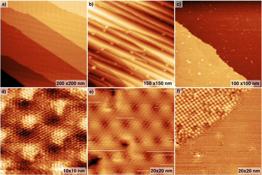
Figure 01. (a) Large STM image showing different terraces and step edges of the Ir(111) crystal covered with graphene. (b) Large STM image showing the surface of a graphene-covered Ir(332) crystal, where the typical step bunching and parallel terraces are resolved. (c) Large STM image showing terraces and step edges of the Ni(111) crystal; the surface is mostly clean except for some patches of NiC₂. (d) Atomically resolved STM image of the graphene layer, where the large periodicity corresponds to that of the gr/Ir(111) moiré pattern. (e) Close-up STM image of one of the terraces of the Ir(332) crystal, where both the moiré pattern and the atomic periodicity are resolved. (f) STM image showing atomic resolution of clean Ni(111) and NiC₂, used for the Fourier analysis of the periodicities.
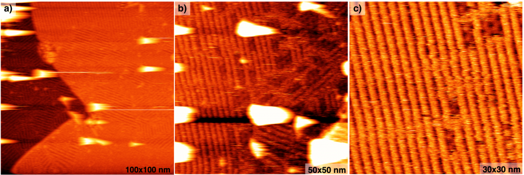
Figure 02. (a) STM image of the gr/Ir(111) surface with a pentacene monolayer. Molecular evaporation parameters: T = 87 °C, t = 1 min. (b) and (c) STM images showing the stripe pattern of the molecular islands. In some patches of the molecular islands, the periodicity of the underlying gr/Ir(111) moiré pattern can be observed.
The second period of the grant (02/2025 – 12/2025) focused on the growth of different transition metal disulfides—MoS₂, VS₂, and WS₂— on graphene covered Ir single crystal substrates. An example of our results of TMDs growth is shown in Figures 03 and 04. Finally, functionalization was carried out, with molecular evaporation, using the protocols that have been developed during first period.
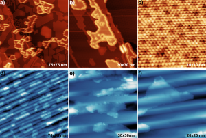
Figure 03: STM characterization of MoS₂ monolayer islands grown on two different graphene-covered substrates. In the case of MoS₂ on gr/Ir(111) (first row), a) provides an overview of the surface, while b) and c) show atomically resolved images where the moiré periodicity induced by the gr/Ir(111) substrate is clearly visible. For MoS₂ grown on stepped gr/Ir(332) (second row), d) and e) present large-area images illustrating the distribution of the islands across the step edges. A close-up view of an individual MoS₂ island is shown in f), revealing continuous growth across the surface without the presence of dislocations.
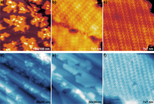
Figure 04. STM images of VS₂ monolayer islands on two different graphene-covered substrates. The first row corresponds to VS₂ on gr/Ir(111): a) overview of the sample, while b) and c) are atomically resolved images, also revealing the charge density wave (CDW) periodicity. The second row shows VS₂ on stepped gr/Ir(332): d) and e) are large-scale images showing the distribution of the islands across the step edges, and f) is an atomically resolved image also displaying the CDW periodicity.
We are currently preparing the manuscript for publication of these final results, and once published, news will be announced here as well.


MOBDOK-2023-4185
DOK-NPOO-2023-10-4241